Showing posts with label amplifier. Show all posts

Tuesday, December 24, 2013

LM4990 2 Watt Audio Power Amplifier with Selectable Shutdown Logic Level

The LM4990 is an audio power amplifier primarily designed for demanding applications in mobile phones and other portable communication device applications. It is capable of delivering 1.25 watts of continuous average power to an 8Ω BTL load and 2 watts of continuous average power (LD and MH only) to a 4Ω BTL load with less than 1% distortion (THD+N+N) from a 5VDC power supply. Boomer audio power amplifiers were designed specifically to provide high quality output power with a minimal amount of external components. The LM4990 does not require output coupling capacitors or bootstrap capacitors, and therefore is ideally suited for mobile phone and other low voltage applications where minimal power consumption is a primary requirement.


2 Watt Audio Power Amplifier with Selectable Shutdown Logic Level  2 Watt Audio Power Amplifier with Selectable Shutdown Logic Level

The LM4990 features a low-power consumption shutdown mode. To facilitate this, Shutdown may be enabled by either logic high or low depending on mode selection. Driving the shutdown mode pin either high or low enables the shutdown pin to be driven in a likewise manner to enable shutdown. The LM4990 contains advanced pop & click circuitry which eliminates noise which would otherwise occur during turn-on and turn-off transitions. The LM4990 is unity-gain stable and can be configured by external gain-setting resistors.
 Features

  • Available in space-saving packages: LLP, Exposed-DAP TSSOP, MSOP, and ITL
  • Ultra low current shutdown mode
  • Improved pop & click circuitry eliminates noise during turn-on and turn-off transitions
  • 2.2 - 5.5V operation
  • No output coupling capacitors, snubber networks or bootstrap capacitors required
  • Unity-gain stable
  • External gain configuration capability

  • User selectable shutdown High or Low logic Level
    Key Specification
    Improved PSRR at 217Hz & 1KHz  62dB
    Power Output at 5.0V, 1% THD+N, 4Ω (LD and MH only) 2W (typ)
    Power Output at 5.0V, 1% THD+N, 8Ω 1.25W (typ)
    Power Output at 3.0V, 1% THD+N, 4Ω 600mW (typ)
    Power Output at 3.0V, 1% THD+N, 8Ω 425mW (typ)
    Shutdown Current 0.1µA (typ)

    Applications

    • Mobile Phones
    • PDAs
    • Portable electronic devices
    Datasheets

    Source: http://www.ecircuitslab.com/2011/07/lm4990-2-watt-audio-power-amplifier.html

    Read More..

    Sunday, April 21, 2013

    Balanced Microphone Amplifier

    We published a design for a stereo microphone preamplifier with balanced inputs and a phantom power supply. The heart of this circuit was a special Analog Devices IC, the SSM2017. Unfortunately, this IC has been discontinued. In its place, the company recommends using the pin-compatible AMP02 from its current product line. However, and again unfortunately, the specifications of this opamp make it considerably less suitable for use as a microphone amplifier. By contrast, Texas Instruments (in their Burr Brown product line) offer an integrated instrumentation amplifier (type 1NA217) that has better specifications for this purpose.


    Incidentally, this IC is also recommended as a replacement for the SSM2017. It features internal current feedback, which ensures low distortion (THD + noise is 0.004 % at a gain of 100), low input-stage noise (1.3 nV/√Hz) and wide bandwidth (800 kHz at a gain of 100). The supply voltage range is ±4.5 V to ±18 V. The maximum current consumption of the 1NA217 is ±12 mA. The gain is determined by only one resistance, which is the resistance between pins 1 and 8 of the IC. The circuit shown here is a standard application circuit for this instrumentation amplifier. R1 and R2 provide a separate phantom supply for the microphone connected to the amplifier (this is primarily used with professional equipment).

    Balanced Microphone Amplifier Circuit Diagram
    Balanced Microphone Amplifier Circuit Diagram

    This supply can be enabled or disabled using S1. C1 and C2 prevent the phantom voltage from appearing at the inputs of the amplifier. If a phantom supply is not used, R1 and R2 can be omitted, and it is then better to use MKT types for C1 and C2. Diodes D1–D4 are included to protect the inputs of the 1NA217 against high input voltages (such as may occur when the phantom supply is switched on). R4 and R5 hold the bias voltage of the input stage at ground potential. The gain is made variable by including potentiometer P1 in series with R6. A special reverse log-taper audio potentiometer is recommended for P1 to allow the volume adjustment to follow a linear dB scale.

    The input bias currents (12 µA maximum!) produce an offset voltage across the input resistors (R4 and R5). Depending on the gain, this can lead to a rather large offset voltage at the output (several volts). If you want to avoid using a decoupling capacitor at the output, an active offset compensation circuit provides a solution. In this circuit, a FET-input opamp with a low input offset (an OPA137) is used for this purpose. It acts as an integrator that provides reverse feedback to pin 5, so the DC output level is always held to 0 V. This opamp is not in the audio signal path, so it does not affect signal quality. Naturally, other types of low-offset opamps could also be used for this purpose. The current consumption of the circuit is primarily determined by the quiescent current of IC1, since the OPA137 consumes only 0.22 mA.
    Author: T. Giesberts
    Copyright: Elektor Electronics
    Read More..

    Saturday, April 13, 2013

    Class AB Power Amplifier Circuit 30w Using Power Transistor


    30W Class AB power amplifier circuit diagram using power transistor. Set the above amplifier up by adjust the variable resistor R1 to maximum and R12 to zero. After this set up is done, the activate / turn on the amplifier. Adjust the R1 so that the measured output offset is between 30 and 100mV. Once set, adjust the R12 slowly to achieve a quiescent current of around 120mA. Keep checking the quiescent current as the amplifier heats up as it might change due to voltage drop changes in the output devices because of the heat. The heatsinks should be 0.6K/W or less for two amplifiers.

    Power supply circuit for 30W class AB power amplifier:
    power supply for 30W Class AB Power Amplifier Circuit
    30W Class AB Power Amplifier Circuit, Link
    Read More..

    Friday, April 12, 2013

    12 VOLT AUDIO AMPLIFIER IC TDA7222AP CIRCUIT DIAGRAM

    12 VOLT AUDIO AMPLIFIER IC TDA7222AP CIRCUIT DIAGRAM


    Note


    Use 12V DC for powering the circuit.

    The IC must be heatsinked.

    Speaker can be a 4 ohms one.

    For optimum performance input and output must be separately grounded.


    Pin Name Description

    1 Vcc Supply Voltage

    2 RR Ripple Reject

    3 MC Muting control

    4 OP AF Signal Input

    5 FB FB Filter

    6 GA Gain adjust

    7 GND Ground

    8 GND Ground

    9 OP AF Output

    10 BS BootStrap

    Read More..

    Monday, April 8, 2013

    2 X 2 4 2 x 4 5 17 Watt Power Amplifier

    Amplifier circuit here is all based on the ic in the gains. Three IC TA7230P, TA7236P, TA7237AP is intregated circuit (IC) which was applied to the power amplifier. Each IC has a different output, different input voltage, all IC TA7230P, TA7236P, TA7237AP is manufactured by Toshiba.


    TA7230P, TA7236P, TA7237AP amplifier schematic
    TA7230P, TA7236P, TA7237AP amplifier schematic
    Read More..

    Sunday, April 7, 2013

    STK013 Amplifier Circuit

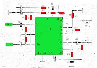
    On the amplifier circuit using ic STK, the same as my previous posting. However, in the above circuit has 2 inputs and 2 outputs, or commonly called a stereo amplifier. This issue of power amplifier 2 x 18Watt and has impedance 8. To stress that it takes about 35-38Volt.
    stk 013 amplifier
    Component list :
    Resistor
    R1 =  390K
    R2 = 390K
    R3 = 220K
    R4 = 220K
    R5 = 220K
    R6 = 220K
    R7 = 100R
    R8 = 1R
    R9 = 9.1K
    R10 = 9.1K
    R11 = 1R
    Capacitor
    C1 = 10uF
    C2 = 10uF
    C3 = 0.47uF
    C4 = 0.47uF
    C5 = 220uF
    C6 = 0.047uF
    C7 = 4700uF
    C8 = 100uF
    C9 = 1000uF
    C10 = 100uF
    C11 = 4700uF
    C12 = 470uF
    C13 = 0.047uF
    IC
    U1 = STK013
    Read More..

    400W High Power Mosfet Amplifier

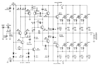
    High Power Amplifier Mosfet 400W . These amplifiers circuit can be used for virtually any application that requires high performance, low use Noise, distortion and excellent sound quality. Examples would be subwoofer amplifier should FOH stage Amplifiers, surround a canal a very powerful sound amplifier, etc. The 400W MOSFET-amplifier has four key stages of amplification. We are looking to start any Phase appropriate detail.

    Schematics Diagram 400W MOSFET Amplifier
    400watt high power amplifier


    As the name suggests All Q ,C and ZD the Bias and buffer phases. Its main goal is to provide a stable MOSFET Gates and offset voltage and the voltage buffer amplifier stage of the High Resource capacity. What would have without the phase response and the effect Slew rate is indeed very bad. The flip side of the coin is not the extra step Introduction of an additional dominant pole in the amplifier feedback loop.

    Also to what the name suggests this stage converts the voltage developed in the VAS and provides all the amps required to drive at 8 or 4 ohms. 2-ohm loads are possible for several minutes at a time. In fact, I have tested more than 1600 1kW amplifier Watts RMS at 2 ohms. But that would not be recommended as a long-term exposure at all. If it is higher than the figures of the STI-amp. Power to the AV amplifier 800 The components of the power for this amplifier are as follows, and are favored A channel or a power module alone. 1 toroidal transformer with a rating of 1kVA. Primary windings are made to fit.
    source:[link]
    Read More..

    Saturday, April 6, 2013

    TBA611 amplifier schematic

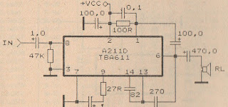
    This amplifier circuit requires voltage ranging from 4Volt to 12Volt, a relatively low voltage. And strong currents needed to obtain a good sound is not too big. This amplifier circuit has a power output or speakers 1W. The output is very small when compared with the voltage amplifiers high. To use it can be used in radio tuner or radio receiver. The series of schemes can be seen below.
    monolithic amplifier with tba


    Technical information
    Vcc                = 4,5-15 V
    Pout               = 1 W
    RL                 = 8 Ohm
    Ft                   = 50-15 Khz
    Icco               = 10 mA
    Package         = TABS4-14
    Manufactered = RFT
    Read More..

    300W subwoofer amplifier schematic

    300W woofer subwoofer systemThis is an amplifier circuit that is formed from a transistor amplifier miraculous. This circuit is used in the speaker subwoofer with 300W maximum power on each side. To apply it, can be used in the room that is not too large, like the car. And the voltage needed between 25 to 42 Volt DC.

    This is schematic of 300W subwoofer amplifier

    subwoofer amplifier circuit rangkaian skematic
    Read More..